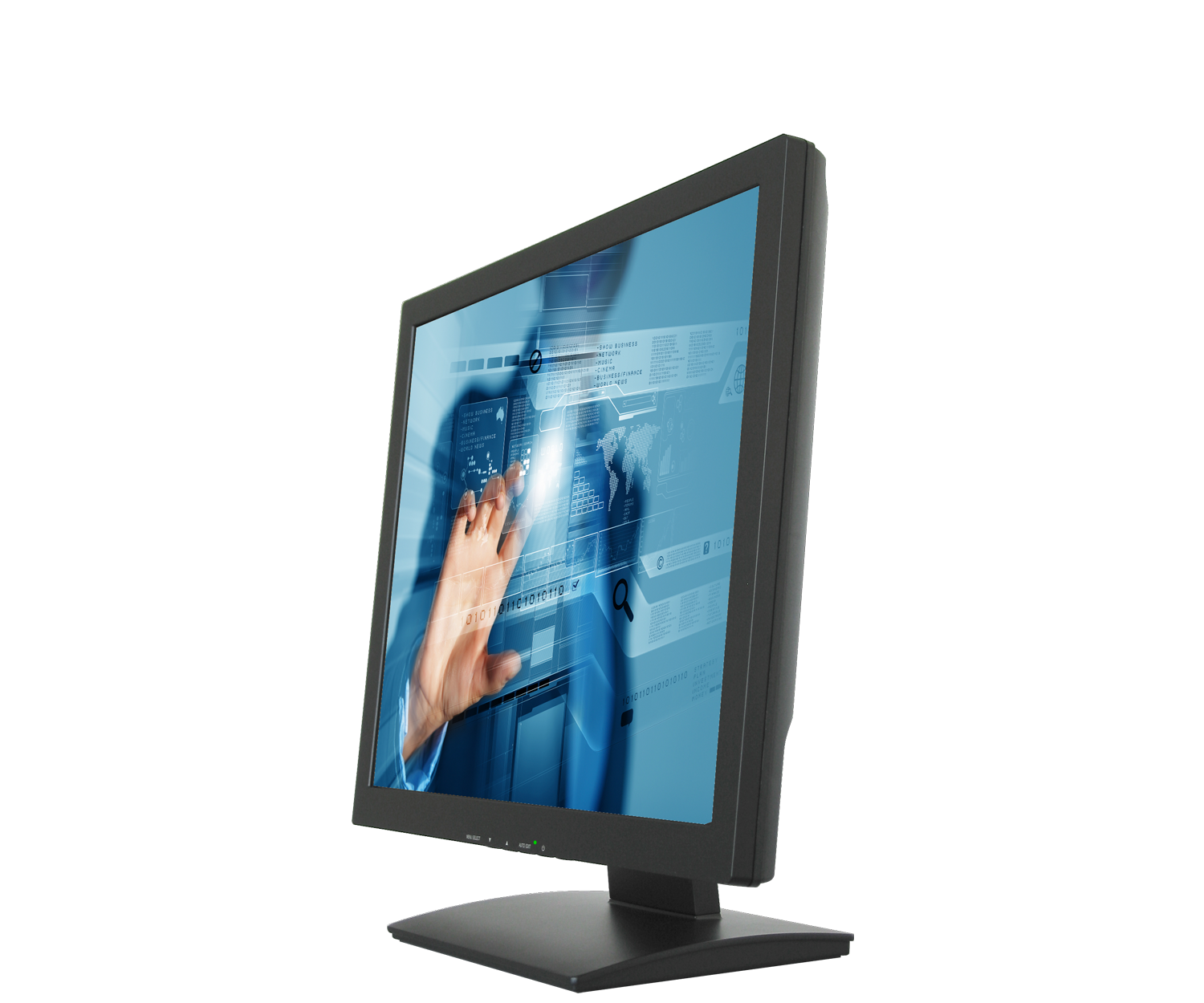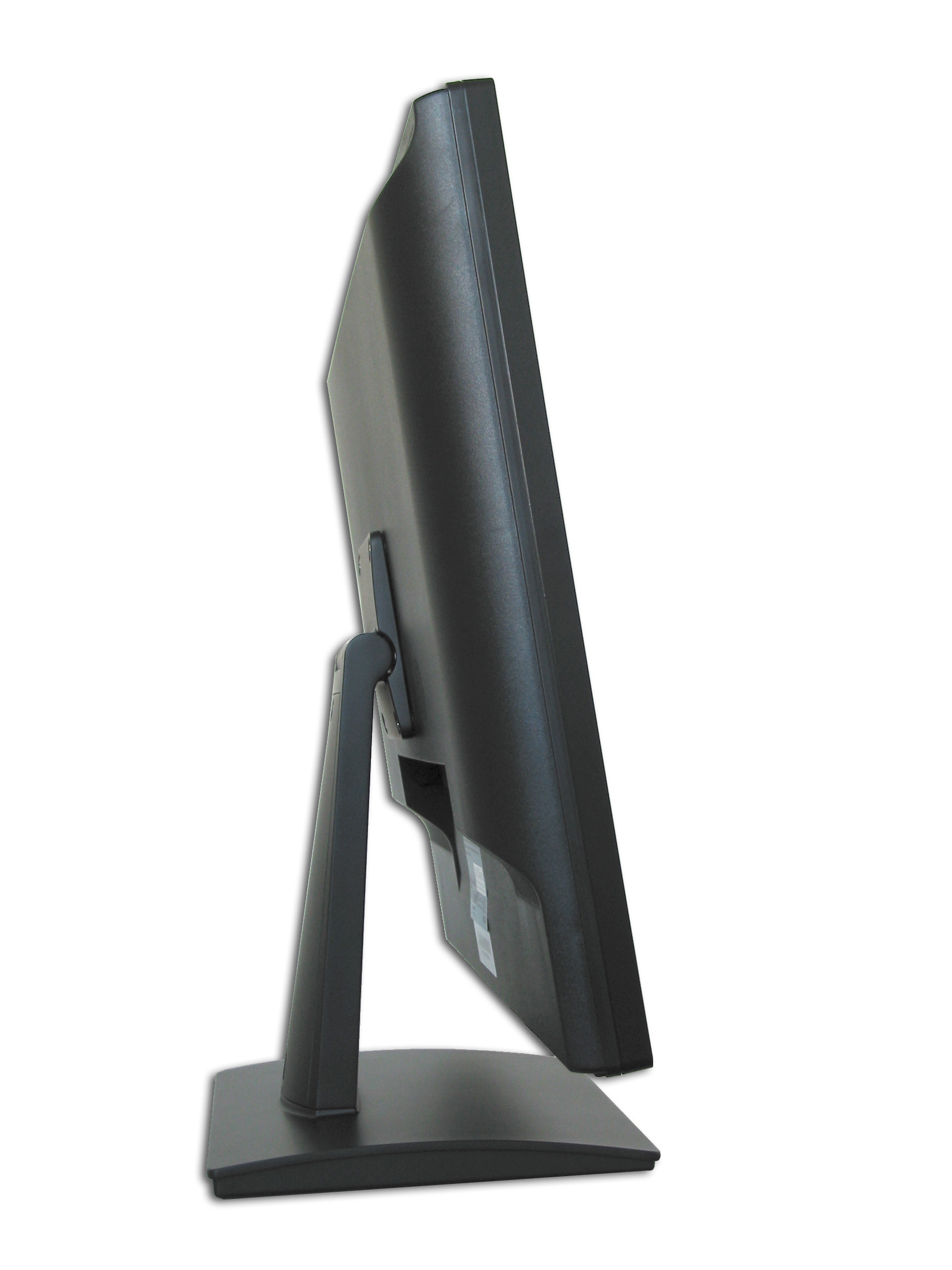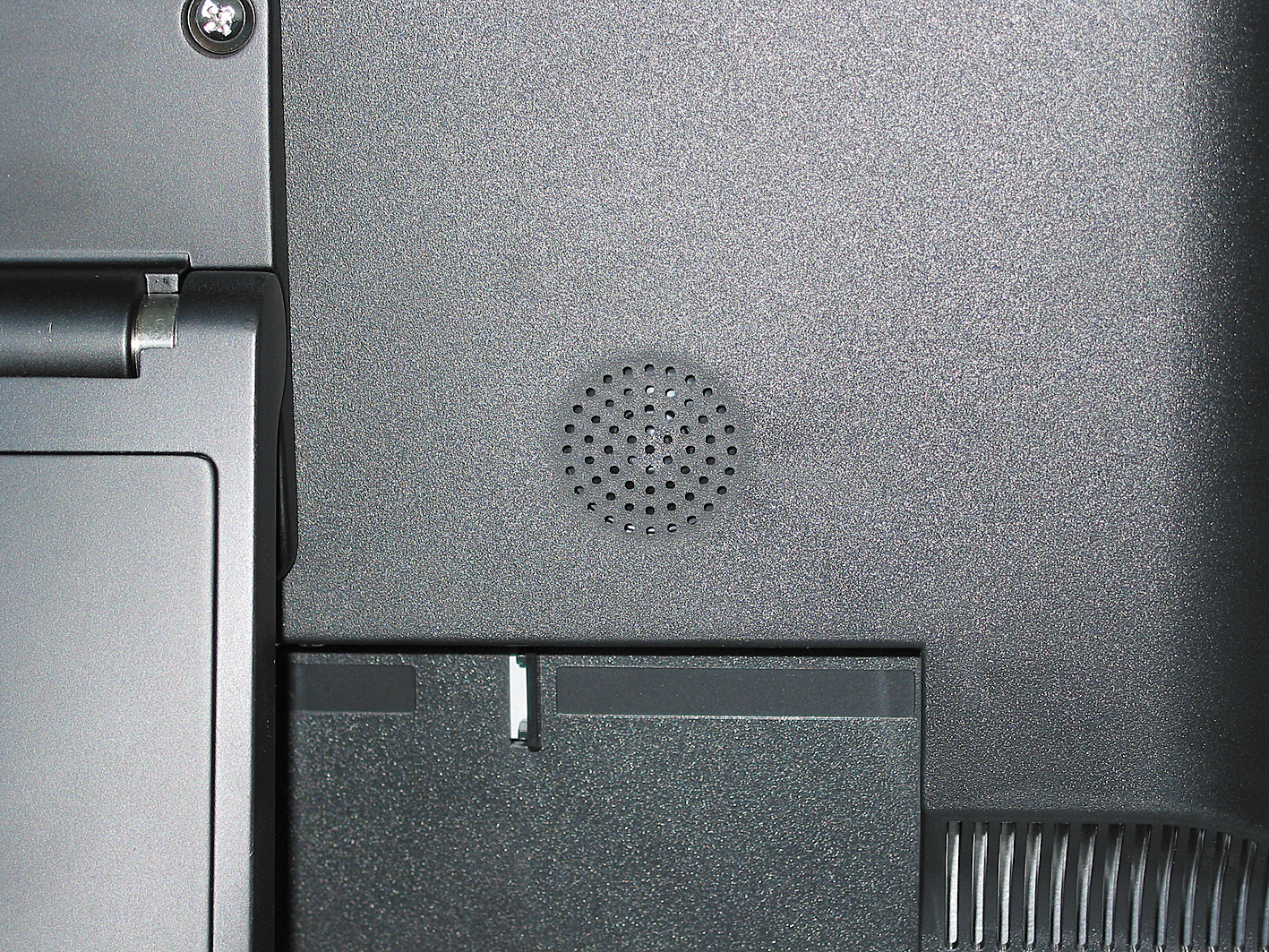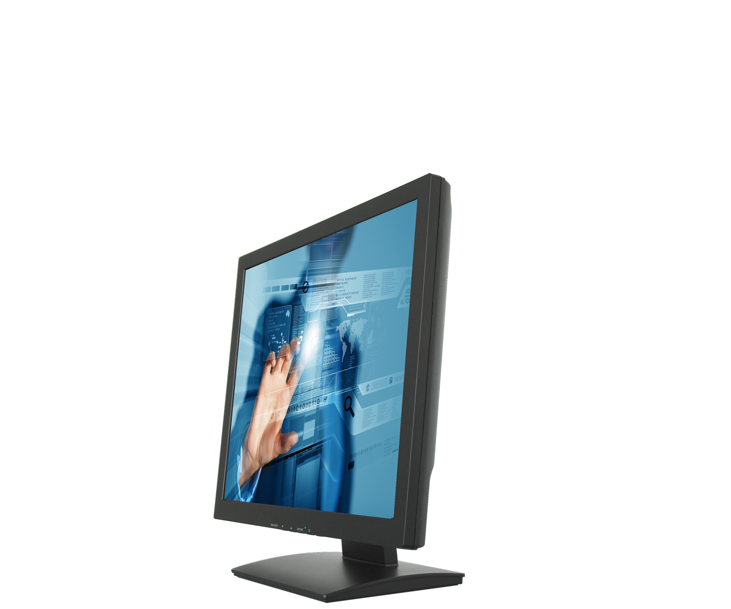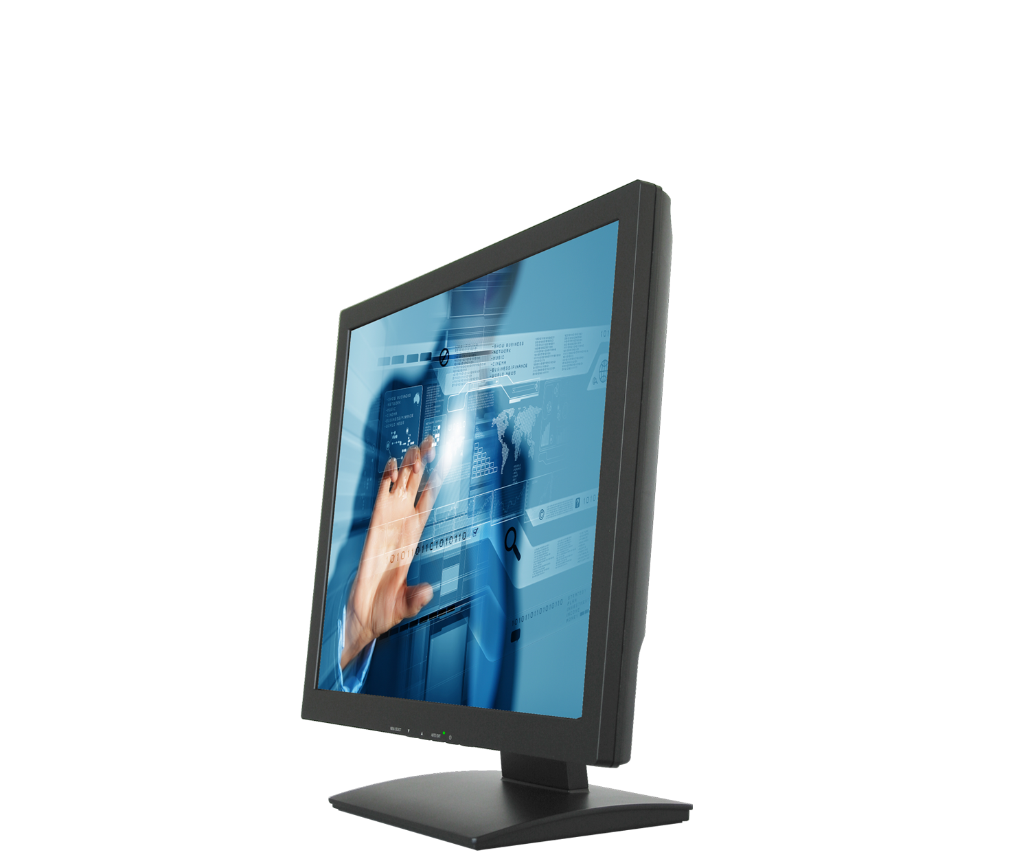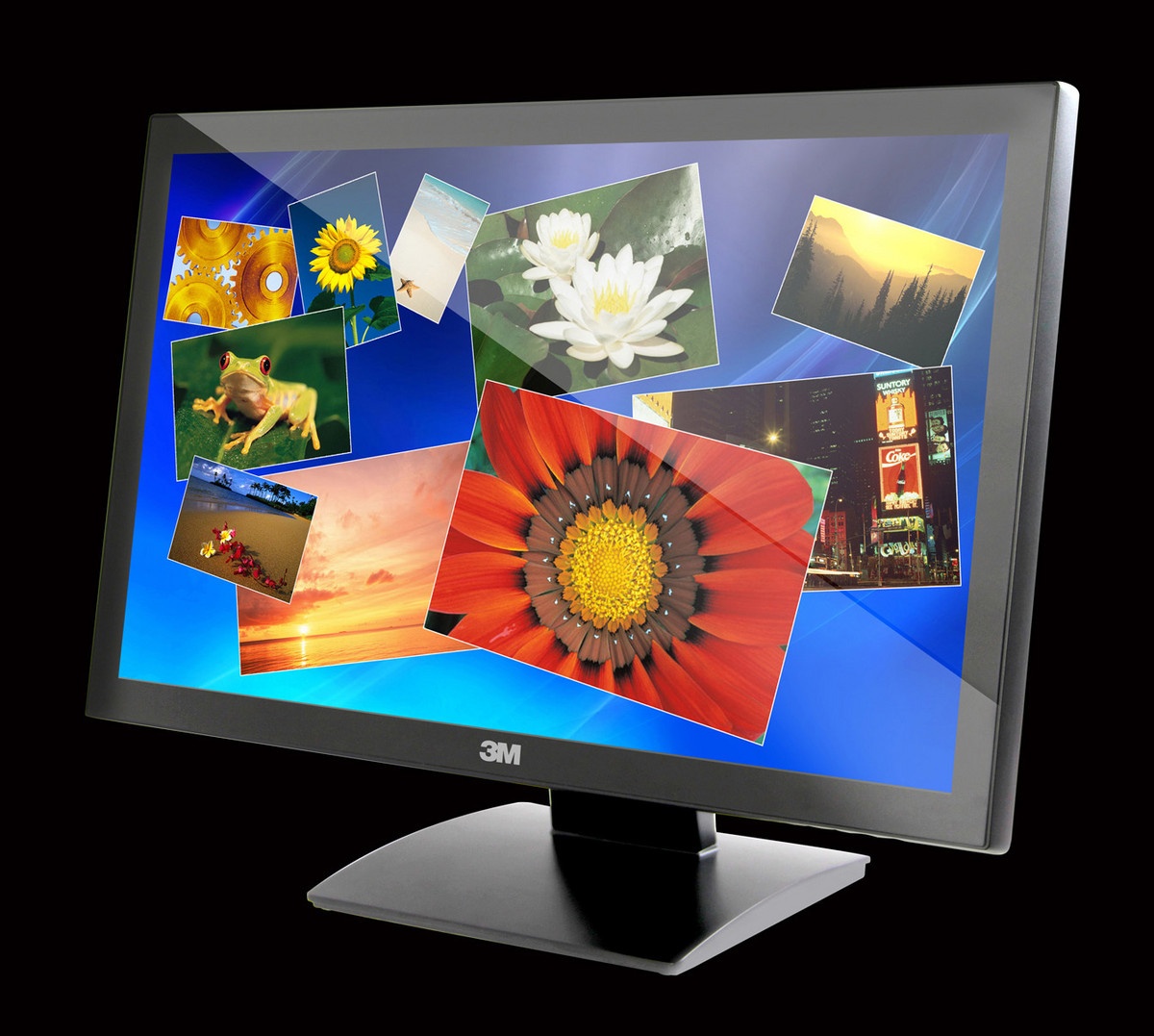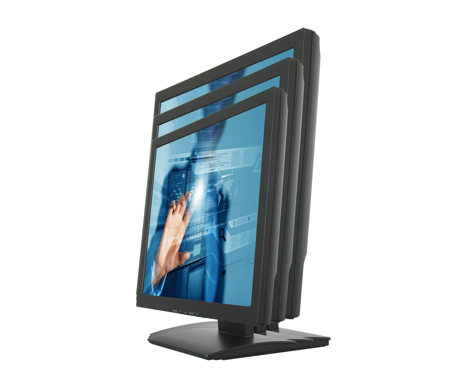
Industrial displays in bezel or True Flat design. Available in 4:3 and 5:4 formats.
- Panel with high Contrast Ratio
- Classic Bezel Housing or True Flat Display
- Resistive Touch or PCAP Touch
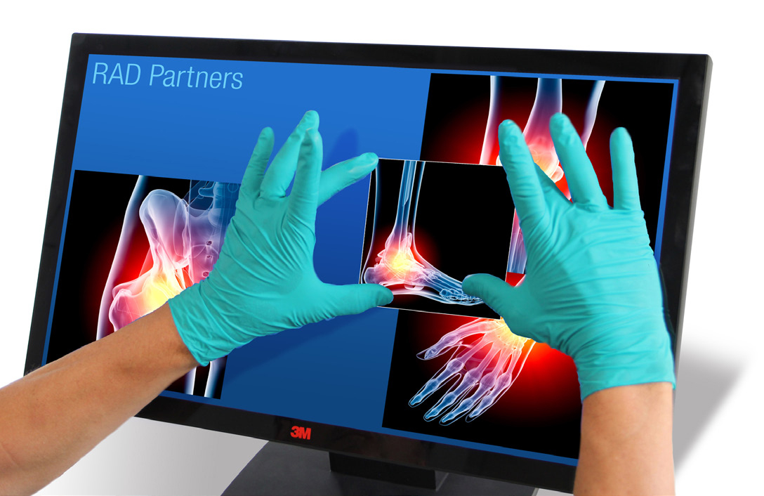
- PCAP Multitouch Sensor with 10 point technology, operable by finger or latex gloves
- OSD Buttons on front side
- VESA compatible
As an OEM/ODM we develop your highly individual monitor solution, starting with the smallest component up to the complex display system.
Every customer has particular needs, depending on the market it serves, and all customers require superior product reliability. Knowing this, Canvys uses a consultative approach and delivers partial to full customized solutions with long-term availability.
After years of partnering with OEMs in industries such as gaming, medical, military/defense, retail, automation/industrial, and transportation, we’re able to bring together the capabilities our customers need:
- Custom engineering
- Strong relationships with key vendors and manufacturers
- Comprehensive solution support
Our ability to successfully serve customers is proven by the number that return to Canvys for the second, third and fourth generation of their solutions.
Available Sizes
Platform Specifications
LED backlight with low power consumption
PCAP Multitouch Sensor with 10 point technology
OSD buttons on front side
Viewing angle of 176°
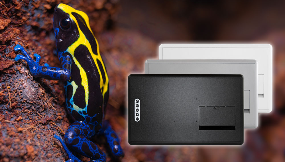
Long-term available plastic housing
| Size | 15″ / 38,1 cm | 17″ / 43,2 cm | 19″ / 48,3 cm |
| Aspect Ratio | 4:3 | 5:4 | 5:4 |
| Recommended Resolution | 1024 (RGB) × 768 (XGA) | 1280 (RGB) × 1024 (SXGA) | 1280 (RGB) × 1024 (SXGA) |
| Display Colors | 16.2M 6-bit 92% sRGB |
16.2M 6-bit + Hi-FRC 96% sRGB |
16.7M 6-bit + Hi-FRC 93% sRGB |
| Panel Brightness | 300 cd/m² typ. | 350 cd/m² typ. | 350 cd/m² typ. |
| Contrast Ratio | 2000:1 typ. | 1000:1 typ. | 1000:1 typ. |
| Viewing Angle (H x V) | 176° / 176° typ. | 170° / 160° typ. | 170° / 160° typ. |
| Housing | Plastic | Plastic | Plastic |
| Certifications and Standards | Safety: cTUVus 62368-1, CB 62368-1,
EMC: EN 55032, EN 55035, FCC Part 15 (Subpart B, Class B) REACH, RoHS, WEEE |
||
Overview of the I/Os
- 1x VGA
- 1x DVI
- 1x USB (Touch)
Detailed Explanation of the Technical Features
Resistive (4-, 5-, 7- and 8-wire)
Sensor Materials
Glass or Acrylic substrate, Spacer dots, Polyester sheet(s)
Principle of Operation
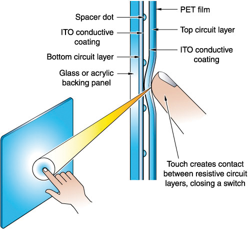
- A touch compresses the flexible Top layer into contact with the bottom glass layer.
- A voltage gradient is applied to the top and bottom layer (X and Y axis) sequentially.
- The controller calculates the X and Y position of the touch based on the voltage gradient applied to one side and using the opposite side as a voltage probe.
Pros and Cons
| Pros | Cons |
| Most widely used touch technology | PET top sheet is highly susceptible to scratches, cuts and cigarette burns |
| Can be activated by bare finger, gloved hand, or stylus | PET layer is a flexing mechanical element coated with a conductive |
| Low cost | Transmission typically in 80 % to 85 % |
| Limited to two resolvable points; three or more resolvable points requires |
Content and images of 3M were reproduced with permission © 3M 2010. All rights reserved.
White Paper Download
White Paper: Canvys Touch Technology Selection Guide (2021)
7.31 MBDownload
Projected Capacitive Touch
Introduction
Projected Capacitive Technology (PCT) is fast becoming one of the most prevalent touch technologies for an expanding variety of applications ranging from consumer devices to commercial applications in retail and gaming signage. Driven by the increasing number of users of touch-enabled mobile devices, consumer and professional expectations for touch applications have moved far beyond single touch requirements into the realm of multi-touch and multi-user capabilities. Since "projected capacitive technology" is a relatively broad term this post explores two of the most prominent sensing methods, "self capacitance" and "mutual capacitance", and the different options within these sensing methods. Each of these sensing methods address different needs and understanding their strengths and capabilities can help hardware and software developers choose the appropriate touch technology for their application.
How Projected Capacitive Technology Works
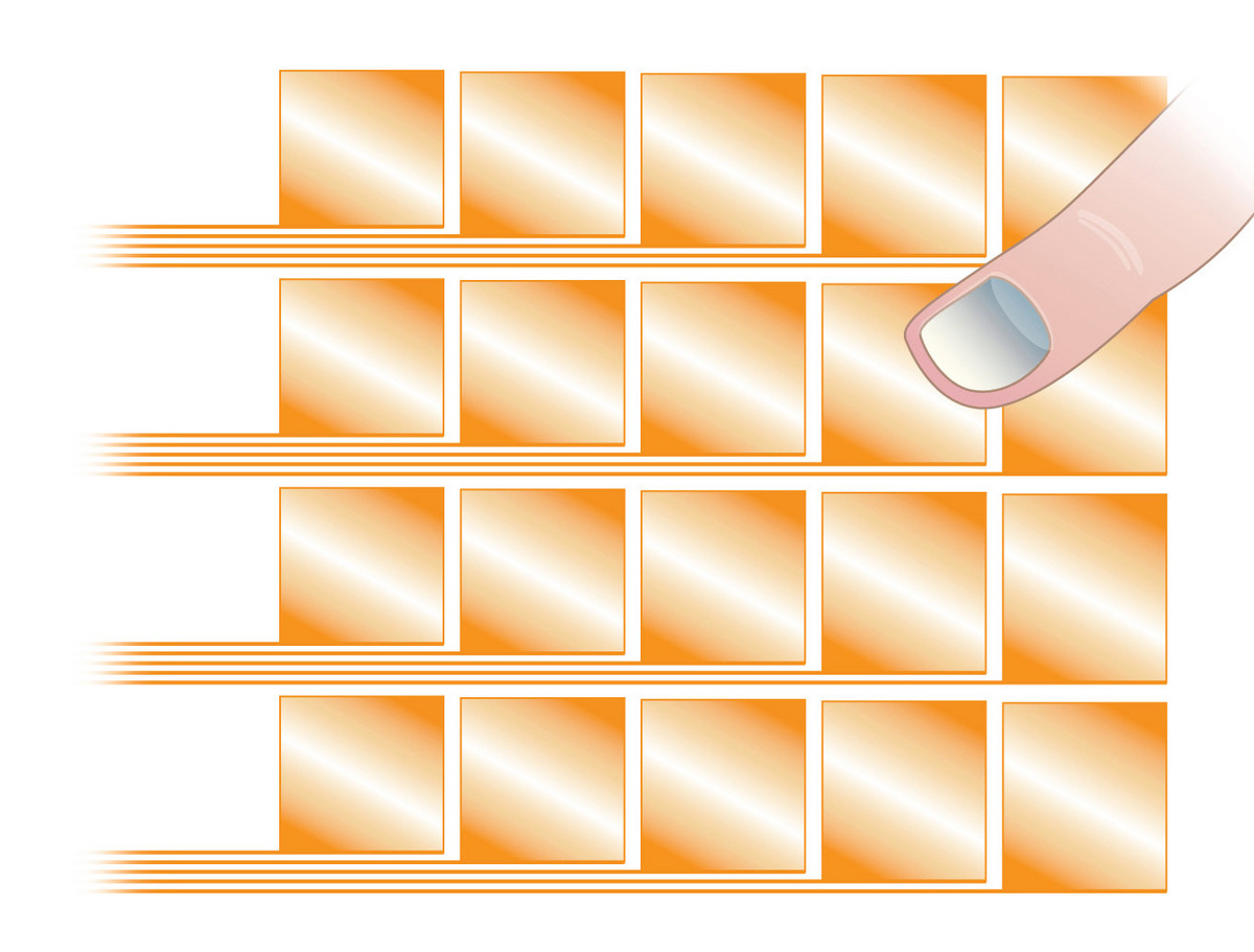
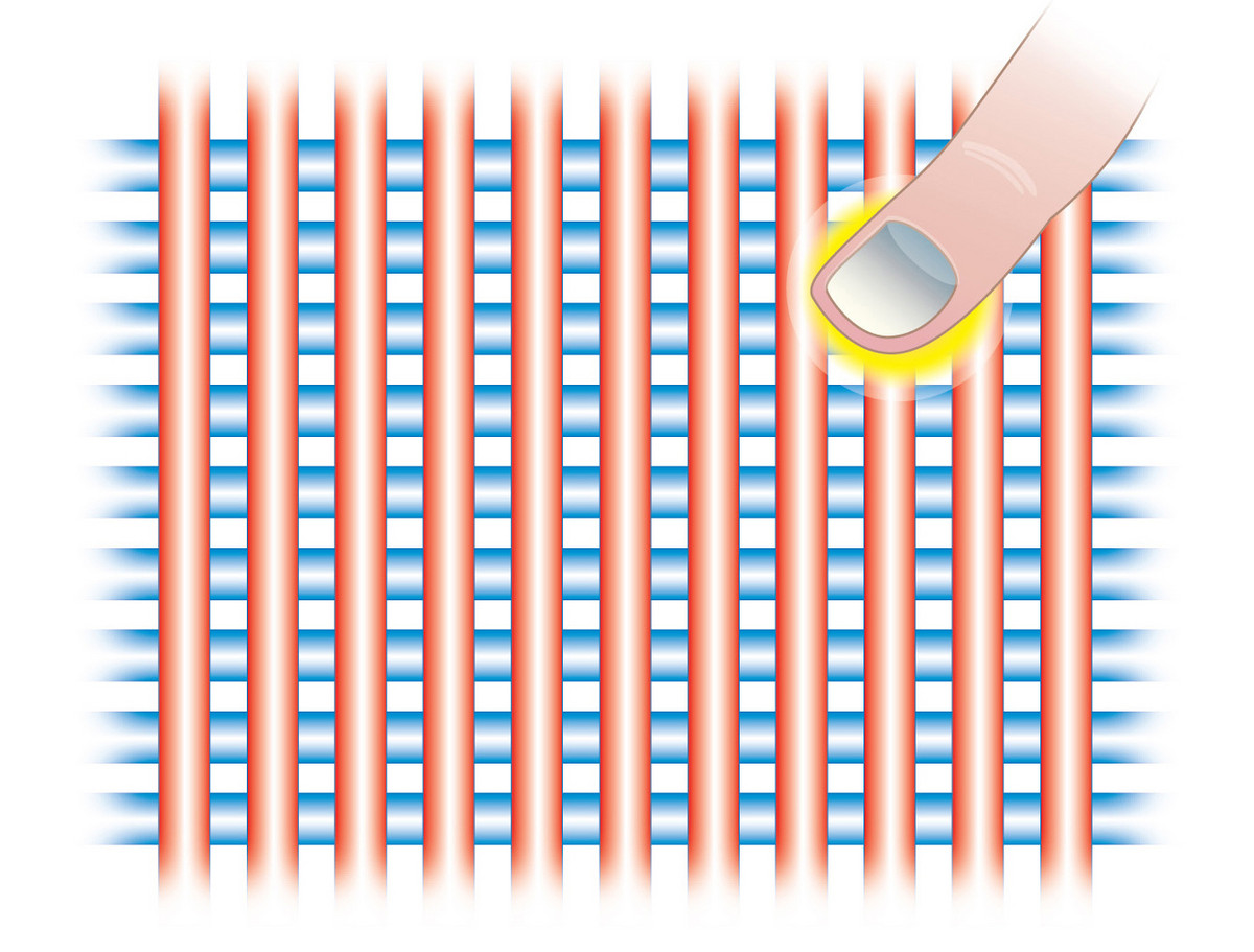
Projected capacitive technologies detect touch by measuring the capacitance at each addressable electrode. When a finger or a conductive stylus approaches an electrode, it disturbs the electromagnetic field and alters the capacitance. This change in capacitance can be measured by the electronics and then converted into X,Y locations that the system can use to detect touch. There are two main types of sensing methods, self-capacitance and mutual capacitance [see illustration 1 and 2], where each has its own advantages and disadvantages.
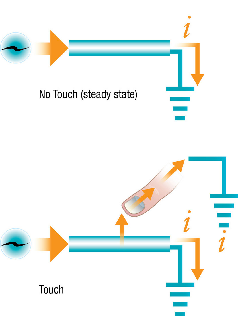
Self-Capacitance
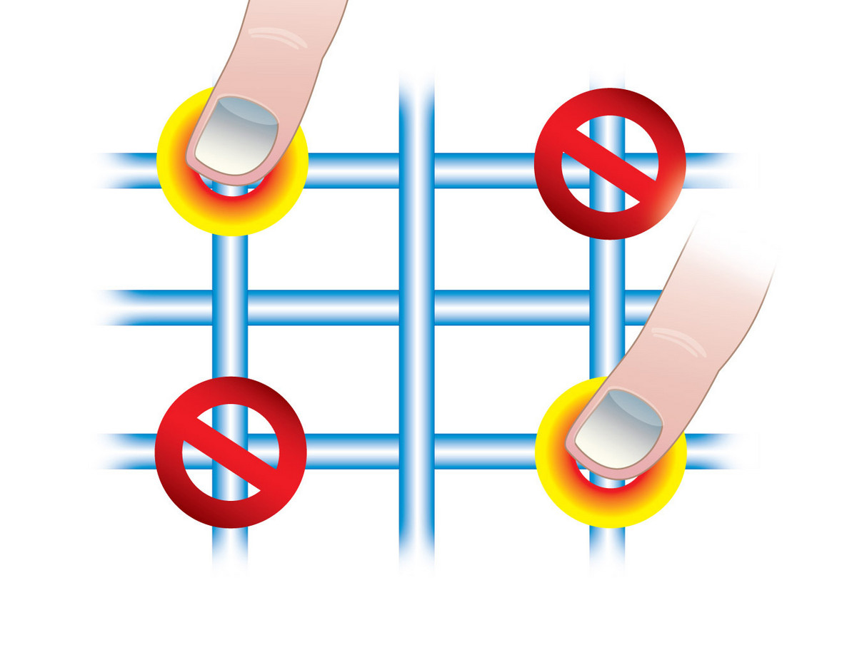
In this implementation, the electronics measure the current on each electrode to ground and therefore is called "self-capacitance". There are two options for how the system can detect touch — multi-pad construction or rows and columns [see illustration 3 and 4]. In a multi-pad construction, each electrode, or "pad", is individually addressable by the electronics requiring an individual connection between the electrode and the controller. This allows multi-pad self capacitance to support greater than one touch, but given that each pad must be individually addressed, it makes the implementation of this solution for screens greater than 3.5 inches very challenging. In a row-and-column construction, each row and column is an electrode and therefore is individually addressed by the controller. Even though the intersection of a row and column represents a unique coordinate pair, the electronics are not able to measure each individual intersection as they can only measure each electrode. This limits row and column self-capacitance implementations to single and dual touch detection where "ghost" points can be a problem. Ghost points are the result of imaginary or false row and column intersections in locations other than the touch location [see illustration 5].
To sense touch in a self-capacitance implementation, the electronics scan through each electrode and measures the amount of current on each electrode to establish a steady-state current. When a finger or grounded conductive stylus approaches the screen, they couple to the electrodes and increase the current draw as it creates a path to ground. By determining which row and column is closest to the touch location, and using interpolation for higher precision, a controller can determine the location of a touch.
Mutual Capacitance
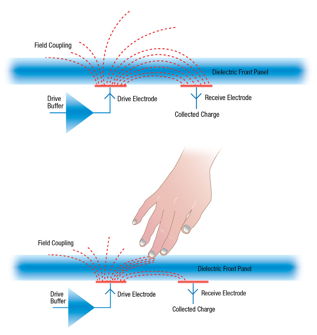
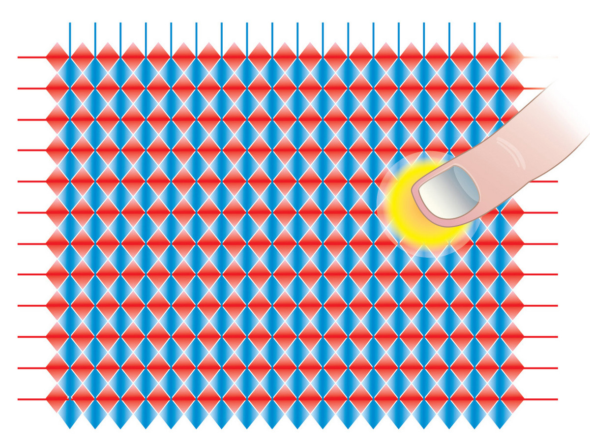
Mutual capacitance is the intentional or unintentional capacitance between two "charge holding objects." Projected capacitance touchscreens intentionally create mutual capacitance between elements of columns and rows [see illustration 6] in the vicinity where each intersect the other. This allows the system electronics to measure each node (intersection) individually to detect multiple touches on the screen during one screen scan.
When a finger touches near an intersection, some of the mutual capacitance between the row and column is coupled to the finger which reduce the capacitance at the intersection as measured by the consystem electronics. This reduced capacitance crosses the "touch threshold" set by the electronics indicating a touch has occurred.
Capacitance Touchscreen Construction
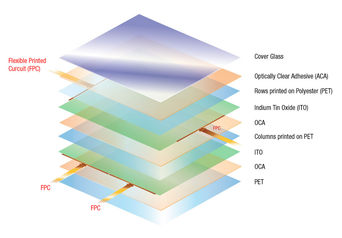
Several techniques are available to construct a capacitance touchscreen. These include conductive wire construction or the application of transparent conductive materials, such as Indium Tin Oxide (ITO), to a polyester (PET) film layer "sandwich" or to a glass substrate.
Conductive Wire Construction
Conductive wire construction provides a greater signal-to-noise ratio than ITO construction. However, the wired lines are typically visible to the naked eye. Wires can be designed into a grid array pattern and separated by a dielectric layer or specially designed for a single layer with a cover glass or PET over the electrodes.
Indium Tin Oxide (ITO)
Indium Tin Oxide (ITO) sputtered onto a surface (glass or PET) achieves a sheet resistance typically in the
50-200 Ω squared range. Sheet resistance and light transmission are directly proportional,meaning that higher resistance equals higher light transmission as the ITO layer is typically thinner when trying to achieve greater light transmission.
Index matching is one way to reduce pattern visibility when using lower resistance patterns. To create the pattern needed for the matrix or diamond design of the capacitance grid, laser etching, photolithography, and many proprietary methods can be used. In row and column ITO implementations, the conductive layers need to be insulated from one another.
Sensor Construction
Polyester (PET) film can be used for projected capacitive in three ways: a conductive pattern printed on two separate sheets and then laminated together; a conductive pattern printed on both sides of a single sheet; or two conductive patterns printed on the same side with a dielectric layer in between with conductive bridges. Single layer constructions can reduce the overall stack up which is important in compact mobile displays, but it requires a double pass (imaging) on the same layer. For a two layer construction only a single pass is required, but the lamination of two layers of PET requires precision alignment [see illustration 7]. On a single sided, double print solution, the bridging pattern can sometimes create optical anomalies that can be seen by the naked eye.
Glass solutions can have similar constructions as that of PET. The benefits of glass are that it can offer improved optics and rigidity. The disadvantage of glass on the sensing layers is that it requires a unique layer image mask for each sensor size or design. This can be a barrier to lower volume production and provides less flexibility on sensor customization and design since the cost of new layer masks can range from $40,000 to $100,000. In addition, a PET construction allows for higher capacity, roll-to-roll manufacturing process which can reduce cost and increase flexibility, while glass-based solutions require individual glass sheets with a limited number of sensors per sheet.
Patterning
Matrix patterns and diamond patterns are most commonly used for manufacturing project capacitive sensors. Diamond ITO patterns can be more uniformly printed than matrix patterns which helps improve optics by reducing the impedance of the printed pattern, which results in improved overall system performance.
Some touch technologies, such as surface capacitive, have a uniform conductive coating on the surface which allows for a uniform transmission constant which is less visible. Even though ITO is a transparent conductive layer, with patterned ITO, the breaks in the pattern can be detected by the user due to changes in light refraction.
In order to reduce the visibility of the pattern, sophisticated index matching is used to limit light refraction so that the pattern becomes nearly invisible.
Optics
Projected capacitive technology can be offered in many configurations. Index-matched ITO patterns on glass or PET can offer improved optical characteristics. In addition, minimizing the air gap between the display and touchscreen or optically bonding the touchscreen to the display are other ways to reduce light refraction. This results in better contrast and improved light transmission between the display and the end user. Sensors with wired construction offer good transmission between conductive elements, but the 10 micron wires (typical) are visible in the touchscreen sensor. On single-sided constructions the bridge pattern may also be seen which can affect the optics.
Number of Touch Points (one, two, multiple)
Projected capacitive technology in varying configurations can support single, dual and multi-touch. Self-capacitance solutions are limited to single and dual touch where gesturing can be achieved, but ghosting effects can occur. Mutual capacitance is capable of full multi-touch interactivity since each node intersection is individually addressable. Windows 7 Touch Logo requires 2-touch performance as a minimum but can support up to 100 simultaneous touch points.
Speed
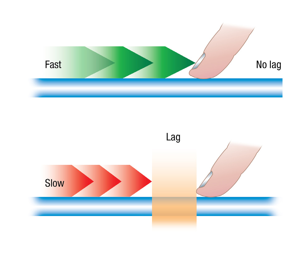
Users are increasingly sophisticated and demand seemingly instantaneous response. Most users are comfortable with a minimum touch response of 20 milliseconds (ms) or less, but experienced users
may be able to detect touch delays of 10 ms or greater. It is important to understand that touch response is not only limited to the touchscreen electronics response time. Application developers must take into account driver delay, operating system delay, software rendering time, and graphics card delay. Minimizing touch response time is an important factor along the entire chain of hardware and software layers, and if the system electronics consumes the entire 20 ms response time needed for optimal user experience, then the total response time can increase to 30-40 ms, thus creating a poor user experience. This response time is often referred to as the "response budget", and this budget of cumulative time delays must be carefully considered in any system hardware/software design solution [see illustration 8].
Different sensing techniques can be used to detect touch and some may provide faster response time. For multi-pad self-capacitance solutions, each pad must be serially addressed which makes it only practical for small display solutions. Row-and-column self-capacitance sensing sequentially scans each electrode to determine touch activation and thus a 40 row by 60 column system would require 100 individual scans.
For mutual capacitance sensing, where each intersection is addressable, that same 40 row by 60 column system would require 2,400 individual scans. This method, known as X/Y, where X represents the rows and Y represents the columns, would dramatically impact response time and make the system unusable. Reducing the measurements to X*1 significantly reduces the measurements by measuring only the number of rows and simultaneously measuring the columns. This results in only 40 measurements for the 40 row by 60 column systems. The disadvantage of this measurement time reduction is a potential for reduced accuracy, so advanced sensing techniques and algorithms are required.
Durability
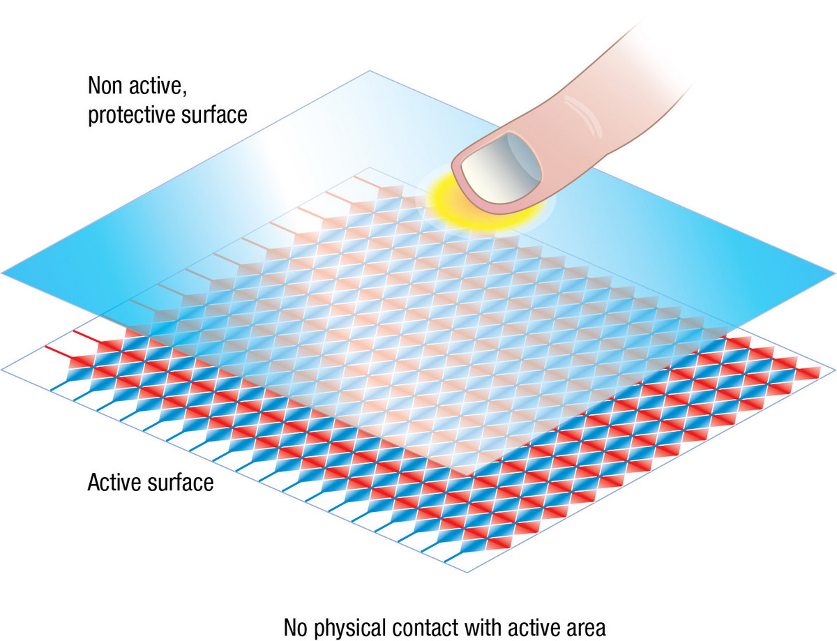
Projected capacitive technology projects a signal outward creating an electrical field that can be measured by the system electronics. This technology does not require direct contact with the active touch surface so a protective cover lens (usually a glass substrate) is often used as the surface of the touch sensor [see illustration 9]. This glass surface can be standard glass, tempered glass, or chemically-strengthened glass depending on the application needs. This "second surface" technology (a front surface that can withstand wear and scratch damage without affecting touch performance) means that screen cracks, scratches or surface wear would have to extend through the entire thickness of the cover glass to reach the electrodes and cause functional damage.
Self-capacitance solutions may have a higher signal level and are typically able to project through thicker cover glass up to 20 mm, although thicker cover glass can affect system performance and accuracy. For mutual capacitance solutions, which has a lower signal level, typical cover glass thickness is in the 0.7 mm to 2.0 mm range.
Transmission (Screen Brightness)
Depending on the sensor's construction, projected capacitive offers different levels of light transmission. For a glass-on-glass solution, light transmission in excess of 90% can be achieved. If PET layers are used, this number may be reduced to 86-90%, however, some advanced processes can achieve greater than 88% transmission using a PET-based construction.
Anti-Glare
Anti-glare characteristics are important in touch sensor design since it allows for optimal screen viewing in ambient light environments.
The reflections on the touchscreen can be significantly reduced by using an anti-glare cover glass. One anti-glare solution is a chemical etch process which creates surface anomalies that refract light, dispersing the light reflection so the user can still see the image on the screen. The second solution is to use a coating applied to the sensor cover glass or to a PET film overlay. Both solutions serve the purpose of dispersing the reflected light to improve the user experience. A heavy anti-glare treatment can negatively impact clarity, so selecting the proper anti-glare solution for a given application is critical.
Anti-Stiction
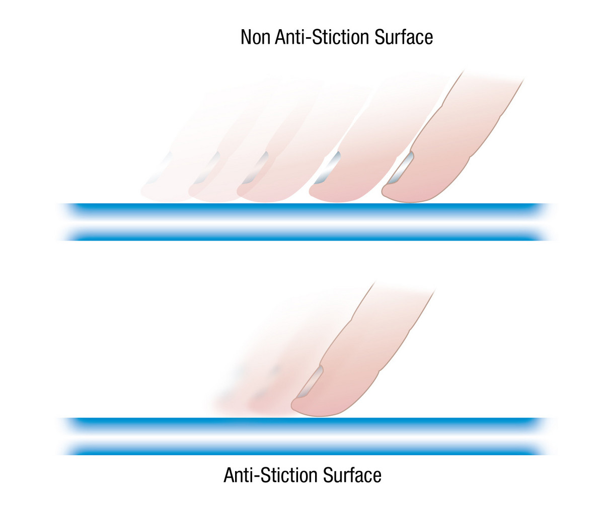
Anti-stiction, meaning the reduction of surface stiction while your finger or object drags on the surface, allows for better user experience. Plain glass and some coatings can increase the friction with as user's fingers during draw, drag, and gesturing applications. With an anti-stiction surface, fingers glide effortlessly across the screen for very smooth, natural gesturing experience [see illustration 10].
Scalability
Inherent in projected capacitive technology construction, scaling larger sensor sizes would require additional rows and columns to maintain the same touch fidelity. Since access to each row and column (electrode) is required, new tail designs and electronics are needed for each design size. In addition, in order to create the new pattern in a glass-based solution, a new mask would be needed to create the unique ITO layers. If conductive wires are used, a new program is required to create the new wire pattern. For PET-based solutions, a new program would be required for singulation of the sensor.
Bare Hands, Latex Gloves and Stylus
Projected capacitive technology's electrical field projects above the cover glass to allow sensing of finger, gloved hands and passive stylus. Self-capacitance systems can be tuned to sense both bare fingers and thick winter gloves, although the ability to sense both under the same setting may reduce accuracy. Mutual capacitance systems can sense bare fingers and thin surgical and food service
gloves, but not thick winter gloves (unless they are conductive gloves). A passive stylus can be designed to work with both technologies, however, the diameter of the stylus tip for a mutual capacitance system can usually be smaller than for a self capacitance system [see illustration 11].
Sensing Lines and Touch Resolution
With projected capacitive technology the number of sensing lines and drive lines determine the number of intersection or nodes. Each of these nodes represent a touch location, plus, by using interpolation,
the system electronics are able to pin-point touch locations by using the information from many of the surrounding electrodes help determine the exact location of touch. Self capacitance sensing is only limited to the information from each row and column scan which provides less information for the electronics to interpolate. Mutual capacitance sensing has a much higher density of electrode information to interpolate, resulting in very high touch accuracy. In the 40 row by 60 column example, mutual capacitive sensing provides
a 24:1 ratio in touch density over self capacitance sensing.
Surface Contaminants
Projected capacitive technology is an ideal solution for contaminant-prone, public access or harsh environments where dust and debris can collect on the surface of the touchscreen or along the bezel edge. Since PCT is unaffected by most surface contaminants, it can be a better self-service technology than alternative touch technologies that rely on sensors at the edge or corners of the touchscreen.
Flat Front Surface, Industrial Design
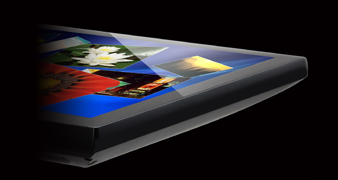
One of the unique features of projected capacitive touchscreens is that the design allows for a flat front surface (FFS) implementation. With all pattern and tail bonds protected by a cover glass, there is no need for a bezel around the screen. This capability allows for enhanced industrial designs that are aesthetically and functionally appealing to the end user. Bezels can keep the finger from reaching the corners of a screen, but in a full screen PCT design the user can access the most extreme corner placements of buttons. In addition, a printed border under the cover glass gives the illusion of a virtual bezel which may be branded with a company's logo or name [see illustration 12]. In addition, utilizing the FFS capability also makes debris build up less likely and simplifies the screen cleaning process.
Product Specifications (typical values)
| Feature | Mutual Capacitance | Capacitance-to-Ground |
| Light Transmission | 84% to 90% | |
| Stylus Type | Finger, Thin Glove, Passive Stylus | Finger, Thin Glove, Passive Stylus |
| Second Surface | Yes | |
| Sealability | NEMA 4 / 12 and IP 65 standards | |
| Response Time | 6 ms | 10 ms |
| Touches | 20+ | 1 (dual) |
| Accuracy | > 99 % | > 98,5 % |
3M...Enabling the Future of Multi-touch
3M’s implementation of projected capacitive technology (3M PCT) is designed specifically for the needs of larger display applications. By maintaining a total solutions focus,
3M has combined decades of film manufacturing technology experience and over 25 years of proven capacitance electronics expertise to create 3M Multi-Touch PCT systems and display solutions ranging in size from 8.4 to 32 inches.
By using a roll-to-roll PET patterning process, 3M is able to provide customers with design flexibility without the high cost of creating new masks for a glass-on-glass solution.
In addition, 3M’s advanced manufacturing process is able to index match the ITO to provide a nearly invisible pattern which, when combined with proprietary optically clear adhesives, gives the touchscreen high clarity and increased light transmission.
With this film-based solution, 3M is able to leverage core competencies in film-based technologies. This will allow 3M to continuously innovate improved coating solutions for better optical characteristics and improve user experiences through enhanced surface feel. In addition, 3M is able to add or substitute layers within the PCT stack to offer additional features, such as light control films for viewer privacy, solar reflection films to help protect LCD's, and safety films to help control glass breakage.
The result of 3M's electronics expertise is the 3M Multi-Touch Electronics PX400, a patented multi-touch controller designed and engineered specifically for this larger display sizes without relying on commonly-used electronics developed for the portable device sizes (3.5” to 11.6”). This optimized controller provides customers with 3M PCT’s unique feature set in a scalable, fully warranted, full multi-touch system solution.
The final key element of the 3M PCT solution is the engineered cover glass. This key element enables leading-edge industrial designs that eliminate surface mount components and bezels which can detract from the overall product aesthetics, be susceptible to damage, and may collect debris. With a non-active cover glass, product designers can extend the touchscreen glass to the display edge and incorporate capacitive, or even mechanical buttons to the industrial design.
The overall result is the 3M PCT multi-touch system, a high performant, high fidelity interactive solution to help meet customers' expanding user interface requirements.
Content and images of 3M were reproduced with permission © 3M 2011. All rights reserved.
White Paper Download
White Paper: Canvys Touch Technology Selection Guide (2021)
7.31 MBDownload
As OEM/ODM we develop your highly individual monitor solution, starting with the smallest component up to the complex display system
With high confidence it is possible to adapt the monitor platform presented here more finely to your individual needs or to the respective application environment. However, there are many possibilities for display customization, which depend on a number of factors. We cannot list everything that is possible at this point.
Therefore we ask you to contact us. Our sales engineers can show you in a non-binding consultation which platform modifications can be realized depending on your specific requirements.
Here is a brief overview of our services and competences with regard to customizing.
Extract from our services regarding further customizing possibilities
Touch Integration
Global value-added touch screen and protective shield integrator of branded and non-branded LCD displays
- Canvys is a global value-added touch screen and protective shield integrator
- Infrared (IR)
- Multi Touch
- Optical (Camera)
- Projected Capacitive (PCAP)
- Resistive (4-, 5-, 7-and 8-wire)
- Surface Acoustic Wave (SAW)
- Surface Capacitive (SCAP)
Looking for 3M Touch Screen Replacements?
Custom Display Enclosures
Canvys offers a variety of custom-built enclosures for industrial and medical applications.
- We utilize only the highest quality materials
- We use injection molding, deep drawing, SLA prototyping, strand-casting, and die-casting
- We offer various housing designs: open frame, panel / chassis / rack mount, customized bezel, back cover design, cable management, rugged housings, slim and light weight designs
- Customer-specific requirements such as a boot logo, back-printed customer logo on the protective glass or touch screen or specific requirements for the respective housing material can also be implemented
- We ensure stable and long-term display availability
As an expert in engineering display solutions, Canvys offers a variety of custom built enclosures for industrial and medical environments.
- We utilize only the highest quality materials
- We use injection molding, deep drawing, SLA prototyping, strand-casting, and die-casting
- We offer various housing designs: open frame, panel / chassis / rack mount, customized bezel, back cover design, cable management, rugged housings, slim and light weight designs
- Customer-specific requirements such as a boot logo, back-printed customer logo on the protective glass or touch screen or specific requirements for the respective housing material can also be implemented
By using long-term available industrial components, Canvys guarantees long-term availability in consistent form, fit and function.
Contact us, we will be happy to assist you in choosing the right housing concept...
Custom Enclosure Options
| Materials | Process / Technologies | Housing Design | Housing Colors | Branding | Protection Class |
| Metal | Injection molded | Customized Open Frame | acerwhite | Customer color | IP Protection up to IP69K |
| Aluminum | Deep Drawing | Customized Panel / Chassis / Rack Mount |
black | Customer logo | |
| Stainless steel | SLA** Prototyping | Customized bezel | gray | ||
| Plastic, UV resistant material like ASA*, Starex | Strand-casting | Customized True Flat Desktop | customized | ||
| Die-casting | Back cover design, Cable management, rugged, slim and light weight designs |
* Acrylonitrile Styrene Acrylate
** Stereolithography
A product will only become a "good product" if it is used successfully in the intended application environment.
When a complex customer project has gone through all phases from start to completion and the customer-specific monitor solution has been manufactured, its true purpose comes into play: Its application!
Only here, in the real operation under realistic environmental conditions, the design, conception, components and the entire system must prove itself. Only if this is successful, our customer will finally speak of success!
Our customer-specific display solutions have been successful for decades in the most diverse applications and markets.

Qualitätskontrolle, -inspektion
Qualitätskontrolle, -inspektion
Ein gutes Qualitätssystem nutzt so viel Feedback wie möglich, um einen Prozess unter Kontrolle zu halten. Bildverarbeitungs-Inspektionssysteme können kritisch sein, wenn es darum geht, prozessbezogene Toleranzen zu überwachen und es den zugehörigen Steuerungssystemen zu ermöglichen, sich an die Toleranzen der Randbedingungen anzupassen.
Global Player/Partner in der Kosmetik-, Lebensmittel-, Pharma-, Körperpflege- und Automobilindustrie nutzen die schlüsselfertigen Inspektionssysteme, um die Qualitätsstandards für ihre Dekorations- und Etikettierprodukte zu erfüllen. Die Systeme untersuchen Etiketten auf Objekten wie Flaschen, Gläsern, Dosen und Behältern - mit bis zu 50 Objekten pro Sekunde.
Aufgrund der langjährigen Partnerschaft mit verschiedenen Unternehmen ist Canvys an der Entwicklung und/oder Änderung dieser Anwendungen beteiligt. Canvys ist vollständig zertifiziert, um Monitore nach diesen Standards zu liefern.
Canvys integriert langzeitverfügbare Komponenten, um die Verfügbarkeit über den langen Lebenszyklus des Produkts aufrechtzuerhalten und zeitintensive Neukonstruktionen und teure Rezertifizierungen zu vermeiden. Zum Einsatz kommen dabei ausgewählte Komponenten ausschließlich von industriellen Roadmaps der Einzelkomponenten. Dies spiegelt sich in den erhöhten Spezifikationen bezüglich Temperaturbereich und Schock & Vibration wieder.
Das robuste Aluminiumgehäuse wurde entsprechend der Anwendung mit IP54-Schutz konzipiert und mit einem frontbündig verklebten Multitouch versehen. Somit ist für zukünftige Bedienkonzepte mit Gestensteuerung schon alles in die Wege geleitet. Die AntiGlare-Beschichtung (AG) des TrueFlat Touchscreen minimiert mögliche Reflexionen der Glasoberfläche und unterstützt die hochauflösende und kontrastreiche Bilddarstellung. Das ergonomische Design der Displays mit integrierter Kabelabdeckung lässt sich problemlos über die VESA-Schnittstelle an bestehende Tragarme einbinden.
Kundenspezifische Anforderungen wie z.B. ein Bootlogo, hinterdrucktes Kundenlogo auf dem Schutzglas bzw. Touchscreen oder spezifische Anforderungen an das Metallgehäuse können ebenfalls umgesetzt werden.
Durch die Verwendung von langfristig verfügbaren Industriekomponenten garantiert Canvys eine langfristige Verfügbarkeit in gleichbleibender Form, Fit und Funktion.
Empfohlene Produkte/Plattformen für diese Anwendung
S SERIE INDUSTRIE-MONITORE
21.5"
OEM/ODM-Plattform mit einem modernen Flachbildschirm und einem robusten Aluminiumgehäuse
- Full HD-Panel mit hohem Kontrastverhältnis
- Modernes True Flat Display für einfache Reinigung und Desinfektion
- Weiter Betrachtungswinkel
- PCAP Multi-Touch-Sensor mit 10-Punkt-Technologie, bedienbar mit Fingern oder Latexhandschuhen
- RFID-Lesegerät hinter dem Frontglas
- All-In-One-Version im gleichen Gehäuse
VA SERIE INDUSTRIE-MONITORE
19"
OEM/ODM-Plattform in Bezel oder flachem Design im klassischen 4:3- und 5:4-Format
- Panel mit hohem Kontrastverhältnis
- Klassisches Bezel-Gehäuse oder Flachbildschirm
- Resistiver oder PCAP-Touch-Technologie
- PCAP Multi-Touch-Sensor mit 10-Punkt-Technologie, bedienbar mit Fingern oder Latexhandschuhen
- OSD-Tasten auf der Vorderseite
- VESA kompatibel
There is currently no further information available on this product.
